ARCHIVE ID
FC-NKT-2024-01
CATEGORY
FutureCircuits
STATUS
Active
CONDITION
Operational
NAKATOMI
Network Architecture Kinetic Assembly Tower Organization Modular Integration
Analysis
NAKATOMI Circuit Analysis Structure
Advanced layer visualization revealing power distribution networks and signal routing across all 32 vertical PCB floors. Diagnostic overlays expose voltage rail architecture and inter-layer via connections throughout the tower structure.
NAKATOMI Circuit Analysis Energy
Standard diagnostic mode displaying the high-rise circuit architecture in its primary operational state. All vertical circuit layers and tower-structured signal pathways visible for baseline analysis of the multi-floor PCB design.
NAKATOMI Circuit Analysis Signal
Internal layer stack analysis exposing hidden copper traces, ground planes, and thermal heat pipe architecture embedded within the multi-story circuit board construction. Critical for examining floor-to-floor interconnect integrity.
Profile
Overview
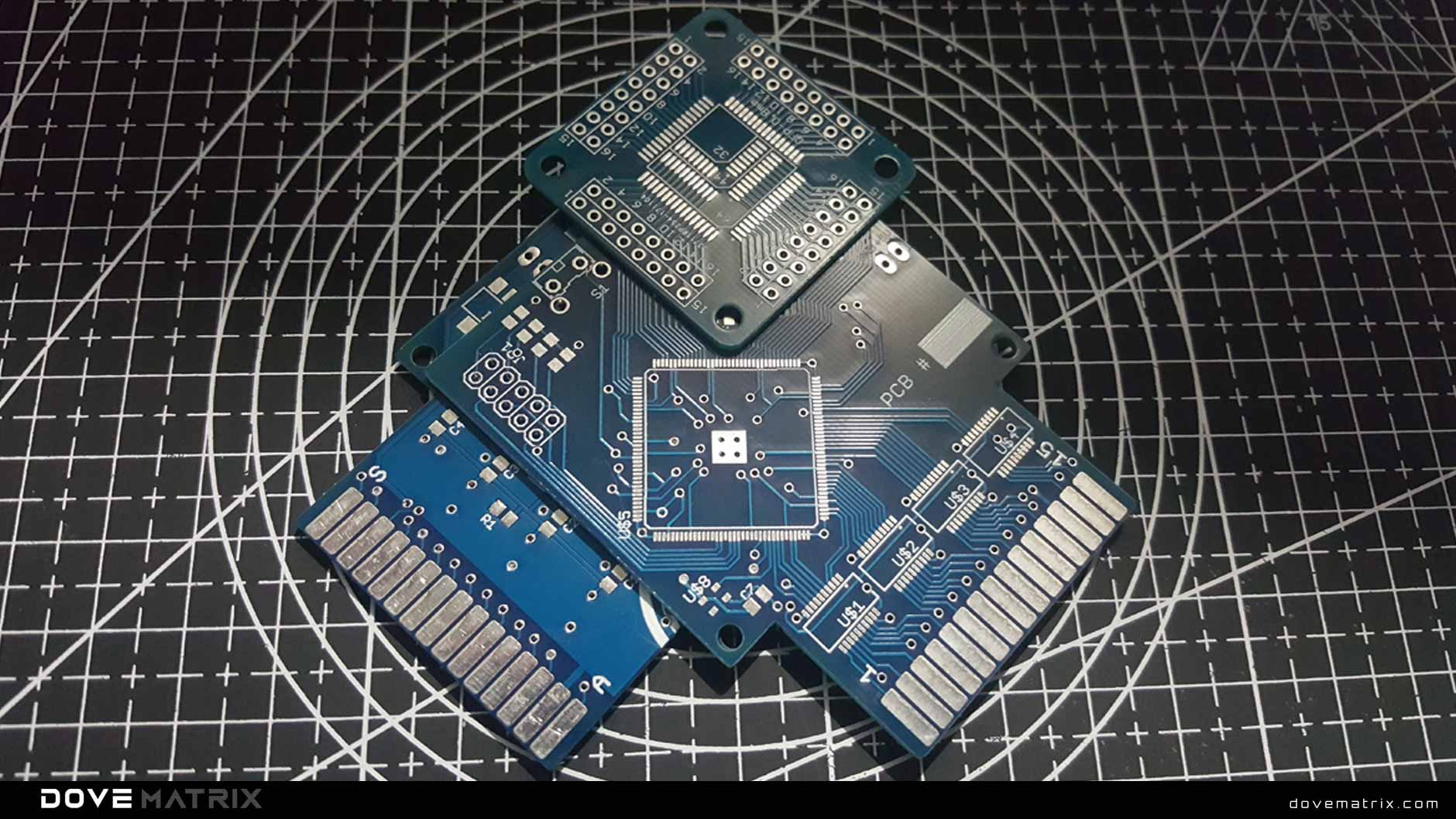
NAKATOMI is a vertically-integrated circuit board architecture inspired by high-rise tower construction, applying architectural principles to maximize component density while maintaining organized signal flow. Unlike conventional flat PCB designs, NAKATOMI treats each layer as a distinct floor in a building, enabling elevation-based functional segregation.
The system employs up to 32 copper layers arranged in a multi-story stack with precision-drilled vias serving as elevators between floors. Core capabilities include high-density component integration maximizing space efficiency, vertical signal routing reducing trace lengths and latency, hierarchical power distribution with dedicated voltage rails per layer, and advanced thermal management using vertical heat pipe architecture to conduct waste heat from internal layers to external dissipation surfaces.
Architecture
NAKATOMI operational architecture implements a floor-based organization where each PCB layer serves a specific functional purpose. Ground planes occupy basement levels providing electrical reference, power distribution layers form mid-level floors with voltage regulation, signal routing layers handle high-speed data transmission on upper floors, and component mounting surfaces cap the structure at penthouse levels.
Vertical interconnection employs strategic via placement acting as express elevators for critical signals and local elevators for intra-floor communication. The thermal management subsystem operates continuously, with heat generated in internal layers conducted through vertical copper pipes to surface-mounted cooling fins. Modular connector systems enable floor-by-floor assembly during manufacturing and provide isolated access points for maintenance and diagnostic procedures.
Behavior
Circuit calibration requires precise alignment of all vertical signal pathways and verification of inter-layer electrical continuity. Primary calibration procedures include via impedance matching ensuring consistent signal propagation across floor transitions, power plane verification confirming voltage regulation at all elevation levels, thermal characterization mapping heat distribution patterns throughout the vertical stack, and signal integrity testing validating high-speed data transmission across multiple layer transitions.
Critical calibration parameters include via resistance maintained below 10mΩ for power connections, signal propagation delay balanced within 50ps across parallel pathways, and thermal conductivity achieving <0.3°C/W junction-to-ambient through the vertical heat pipe network. Environmental considerations include maintaining controlled impedance across the 32-layer stack and ensuring proper ground plane stitching to prevent EMI radiation from the compact vertical architecture.